the aim of this experiment was to see if it was possible to make a simple interface between an
MMC / SD card and the 1802 HHC using its existing serial connection and as few additional components as possible
the memory cards support two communication methods - a fast card-specific bus using a protocol which
employs unique card addressing - and a slower but simpler method using the SPI bus protocol which allows either MMC or SD cards to be used (with a slight modification of initialisation code)
since the description 'slow but simple' could also have been invented to describe the author, i opted for
the SPI bus method
multiple cards can be connected to either type of bus - in the SPI mode, selection of the required card is made using a separate
chip select connection on each card
- the circuit shown here only provides for connection of 1 card at a time
although the code and circuit specifics may apply only to the 1802 HHC, i hope to give enough general information to enable others to adapt the approach to their own particular system, if they wish
hardware details
the 1802 MMC / SD interface circuit
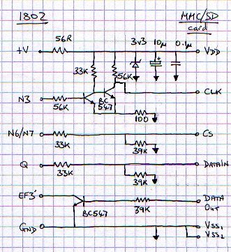
the first thing to note is that the MMC
/ SD cards operate at a lower voltage than the 5v level usually required in CMOS or TTL digital ciruits - the storage card power supply is derived from the 1802 backplane voltage via a resistor and zener diode to provide the 3.3v required for
this circuit
an electrolytic capacitor and a smaller value non-polarised capacitor help to decouple the supply against noise and any effects of a card switching between sleep and active mode (typically
40uA / 40 mA current consumption respectively)
there are two connections on the card which must be connected to system ground
data and control levels are adjusted to produce suitable voltages on either side of the interface
the resistor values shown here on the card Data In and chip select lines
have been selected to convert the HHC output data level '1' voltage to 3.2v approx -
these values will have to be re-calculated for different 1802 systems
the card chip select is controlled using a handshaking line i provided on the HHC serial port:
Output 6 sets the output from a simple Flip-Flop gate and Output 7 resets it
Data Out from the cpu to the card is provided by the Q output
the card clock signal is provided by an Output 3 instruction generating an N3 signal - this is then passed through a two transistor switch (Schmitt trigger) to sharpen up the signal edges close to the card, adjusting the 'high' signal level
to 3.3v in the process
the Data Out from the card to the cpu passes through a single transistor stage which inverts the signal and converts the card output 'high' level to that of the HHC EF3 input
- the collector load resistance for the transistor is supplied by a 47K
pull-up resistor connected to the serial input line inside the HHC
the signal at the HHC 1802 /EF3 pin is buffered via a Schmitt inverter gate, so the
card Data Out signal will have been inverted three times between card and
the cpu's internal input register - therefore the software needs to invert the data sense one more time when it's monitoring the data from the card
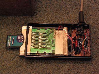
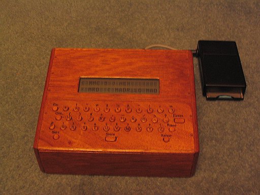
MMC / SD card slot (salvaged from dead PCMCIA
multi-card adapter)
now gaining new life with the 1802 interface
software details
data bytes can be exchanged between cpu and card using a hardware serial I/O
device if it can generate a signal to software to indicate when the 8th bit
of each byte has been received / sent and if the clock signal can be sent
to the card
alternatively, the data can be transmitted on a bit-by-bit basis under direct software control - this is the method
used here since it required minimal disruption to the existing HHC circuitry
since the HHC uses Forth both to develop and to run programs, the
software examples here are given in that language (a homebrew Forth 79
with FIG Forth additions) - individual routines are explained below,
followed by a link to a source listing page
there are three short machine-code routines (two are very short!) shown
both in Forth and regular assembler syntax, the remaining 6 definitions are threaded code
i've tried to provide sufficient description of the routines to enable
the design to be ported to another language if required
so - looking at the code in more detail...
the lowest-level routine 'spi' converts a data byte for transmission to the card on a bit-by-bit basis, msb first - at the same time reading each data bit received from the card (also msb first) to reconstruct the associated input byte
(in practice, useful data is never sent in both directions
simultaneously in SPI mode - dummy bytes of 0FFh are sent from one end
when reading actual data from the other end)
to exchange bytes between the cpu and the card via the SPI bus:
- the output byte is shifted left so that DF is set to the state of the
next bit to send
- the Q output is set or cleared to match DF
- the current value of the input byte is shifted left ready for the next input bit
- the LSB of the input byte value is set or cleared according to the
state of the EF3 input
(in this cct, a '1' level output by the card appears as a '0' on the
EF3 bit of the 1802's internal input register)
- the card clock line is set to '1' for the duration of one Output 3 instruction
- repeat these steps for each of the 8 bits to send/receive
the SPI exchange byte routine is defined as follows:
code spi ( tx_byte -> rx_byte )
\ NB: stack 's' is r3 (&X reg)
rb pop,
\ fetch output byte from stack
00 ldi rd phi rd plo
\ clear value for input byte
08 ldi rc plo
\ set bit counter to 8
here
\ for each tx/rx bit...
rb glo shl rb plo
\ shift tx byte msb into DF
here 04 + bdf req skp seq
\ if next tx bit is '1' then
\ set Q otherwise clear Q
rd glo shl
\ shift input byte left
here 04 + b3 01 ori rd plo
\ if next rx bit is '1' then
\ set bit in input byte
s dec 03 out
\ pulse N3 o/p to clock card
rc dec rc glo
\ ...repeat for next bit
bnz
rd push,
\ push input byte to stack
next
end-code
here is the equivalent routine in a
regular assembler format:-
; r3 is 'X' reg on HHC, re-assign to suit, if required
;
spi
ldxa ; fetch output byte parameter from 'stack'
phi rb ; -
ldxa ; -
plo rb ; - replace with
preferred parameter passing method
ldi 00
phi rd
plo rd
ldi 08
plo rc
nextbit
glo rb
shl
plo rb
bdf outdata1
req
skp
outdata1
seq
glo rd
shl
b3 indata0
ori 01
indata0
plo rd
dec r3
out 3
dec rc
glo rc
bnz nextbit
dec r3 ; store rd as input
byte parameter on 'stack'
glo rd ; -
stxd ; -
ghi rd ; -
str r3 ; - replace
with preferred parameter passing method
sep r8 ; return to Forth
inner interpreter
; - replace to suit system, if necessary
things to note:-
- some cards clock both input and output data on rising clock edge ...and some appear to clock output from
the cpu on rising edge and output from the card on falling edge
- you may need to experiment with
the shift / test / clock order of transmitting and receiving data bits
if your received data is displaced by 1 bit
the low-level I/O routine, 'spi', is used to define a routine ('mmc') which will send properly formatted commands to the card
the MMC commands used here are:-
CMD0 - Reset card (& enter SPI mode)
CMD1 - Poll card initialisation state
CMD17 - Read a single data block from the card
CMD24 - Write a single data block to the card
the MMC command sequence consists of 6 bytes:-
byte 1: command byte (MSB=0, next bit=1,
bits5-0=command no. in binary)
bytes 2-5: 32 bit argument (=0,0,0,0 if not required)
byte 6: CRC (=95h for CMD0;='don't care' for all other SPI
commands)
eg.
40 00 00 00 00 95 (Reset card)
51 01 23 45 00 FF (Read data block from byte address
01234500h on card)
after receiving a command, the card will reply with a response byte (00=completed ok; bit
0=1 means still busy; bits 1-6=error bits:
refer to the MMC standard or a card user
manual for further details)
the 'mmc' routine operates as follows:-
- the 4 argument bytes are stored into the 6 byte command buffer 'cmd'
- bit 6 of the command byte is set and the byte is stored in the buffer
- each byte is fetched in turn from the buffer and sent to the card
- up to 8 bytes are then read from the card - any non-0FFh byte received
within this loop is returned by the routine as the card response to the
command, otherwise 0FFh is returned to indicate no response was received
hex
variable cmd here 2- dp +! ( 6 byte command buffer )
40 c, 00 c, 00 c, 00 c, 00 c, 95 c,
: mmc ( command arg_lo arg_hi -> response )
cmd swap over 1+ ! \ store arg bits 31-16
swap over 3 + ! \ store arg bits
15-0
swap 40 or swap c! \ store command byte with bit 6
set
cmd 6 + cmd
\ for each byte in command buffer...
do
i c@ spi
\ fetch byte from memory and send,
drop
\ ignore input byte
loop
0FF
\ set initial dummy tx byte to 'all 1s'
8 0
\ for up to 8 rx bytes...
do
spi dup 0FF = not \ ...read next byte from card
if leave then \ if rx
byte not 0FFh then exit loop
loop ;
the mmc command routine is used to define higher-level card operations:-
- card initialisation
- read card data into RAM
- write RAM data to card
to initialise the MMC card after power-on, or insertion:-
- the chip select line is raised to '1'
- 10 bytes of 0FFh are sent to the card
- the chip select line is dropped to '0'
- a CMD0 reset command sequence is sent to the card
- if a response byte of
01h is received, continue with next step,
otherwise abort and retry
- poll the card with the CMD1 command sequence for up to 8 attempts
- as soon as a response byte of 00h is received continue with next step,
otherwise abort and retry
the card chip select control is defined as follows:-
code N6 ( -> )
s dec 6 out next \ Output 6 to raise card chip select
end-code
code N7 ( -> )
s dec 7 out next \ Output 7 to drop card chip select
end-code
here is the equivalent code in a regular assembler format:-
N6
dec r3
out 6
...
N7
dec r3
out 7
...
\ the following two definitions each send a dummy byte
\ to the card after changing the chip select state to
\ allow the card to complete any previous operation
: ccs0 ( -> )
N7 0FF spi drop ; \ drop chip select and send dummy byte
: ccs1 ( -> )
N6 0FF spi drop ; \ raise chip select and send dummy byte
the card initialisation
routine is defined as follows:
: mini ( -> )
ccs1
\ raise card
chip select
0A 0 do 0FF spi drop loop
\ send 10 0FFh bytes to card
ccs0
\ drop card
chip select
0 0 0 mmc
\ send CMD0 reset sequence
dup 01 =
\ if card response is 01h...
if ( true ) 8 0
\ ...send up to 8...
do drop 1 0 0 mmc dup 00 = \ ...CMD1 poll sequences
if leave then
loop
\ if card didn't return 00h...
?dup
if ." mmc init err:" . abort
\ ...report init. error value
then
else ." mmc reset err:" . abort \ report reset error value
then ccs1 ;
\ raise
chip select on exit
to read data from the card:-
- prepare the 32 bit argument with the card data start address
- drop card chip select
- send CMD17 block read command sequence
- receive and check for valid response byte from card
- check up to 8 input bytes for data start token 0FEh
- receive full block of data from card
- receive and discard two CRC bytes from card
- raise card chip select
the read card data block routine is
defined as follows:
: mrd ( madr_lo madr_hi
adr -> )
ccs0
\ drop card chip select
rot rot 11 rot rot mmc dup \ send CMD17 block read to card
if ." mrd err:" . abort \ if command failed ...report error
else ( 0 ) 8 0
\ ...otherwise read up to 8 bytes
do 0FF spi 0FE =
\ if input byte is 0FEh...
if drop 1 leave then
\ ...exit from loop
loop
\ loop back for next byte
if xfrlen over + swap
\ if no errors...
do 0FF spi i c! loop
\ ...read all data into memory
0FF spi drop 0FF spi drop \ discard two CRC bytes
else ." mrd timeout" abort \ ..else report error
then
then ccs1 ;
\ raise card chip select
to write data to the card:-
- prepare the 32 bit argument with the card data start address
- drop card chip select
- send CMD24 block write command sequence
- receive and check for valid response byte from card
- send dummy byte (0FFh) to card
- send data start token 0FEh to card
- send full block of data from card
- send two dummy CRC bytes to card
- receive and check data valid token from card
- wait for 'busy' tokens from card to finish
- raise card chip select
the write card data block routine is
defined as follows:
: mwr ( adr madr_lo madr_hi
-> )
ss0
\ drop card chip select
18 rot rot mmc dup
\ send CMD24 block write command
if ." mwr err:" . abort \ if command failed ...report error
else drop
\ ...otherwise...
0FF spi drop
\ send dummy byte to card
0FE spi drop
\ send data start token to card
xfrlen over + swap
do i c@ spi drop loop \ send full data block to card
0FF spi drop 0FF spi drop \ send two dummy CRC bytes to card
0 4 0
\ read up to 4 bytes from card
do 0FF spi 0F and 5 = \ if data valid token received...
if drop 1 leave then
\ ...exit from loop
loop
if 80 0
do FF spi
\ if no errors...
if leave then
loop
\ ...wait for busy token to finish
else ." mwr failed" abort \ ...otherwise report error
then
then ss1 ;
\ raise card chip select
if you build this, or similar, MMC interface for an 1802 system
with Forth and actually want to try out the code given here...
(is this a good time to mention also that you do so entirely at
your own risk?)
to initialise the MMC card:-
- power up the 1802 system with MMC interface circuit connected
- insert MMC card into slot
- enter 'mini'
- if Forth responds 'ok' proceed to a test read
- if you got an error report instead...
...welcome to the wonderful world of hardware & software debugging!
to read data from the card (following successful initialisation!):-
- enter '0 0 bbbb mrd'
(where 'bbbb' is the RAM address of a 200h byte buffer)
- if Forth responds 'ok' check out a dump
of the buffer contents
- a Windows compatible format on the card will show standard 'boot
sector' contents, probably starting 'F3 33 C0...' and some boot error
message text towards the end of the buffer, eg. "Invalid partition
table..", etc
(if you were thinking of ever booting DOS
or WIndows from the card into your 1802 system ...or even into a Windows
PC... you might want to replace the '0 0' in the next test with
the address of a card sector which you can overwrite without losing too
much sleep)
to write data to the card (following a successful read!):-
- enter 'bbbb 0 0 mwr'
(where 'bbbb' is the RAM address of a 200h byte buffer containing
recognisable data content ...i hear that 'Hello World' is out of
copyright now, and back in the public domain)
- if Forth responds 'ok', read the block
back into a different RAM buffer and confirm that the write was indeed
successful - if it was, you will probably do as i did in the same
situation and utter a short burst of static, quickly followed by 'thank
you, thank you, thank you' to St Babbage, the patron saint of computing
the definitions given on these pages provide enough functionality to initialise an MMC card and read or write data between the card and
the 1802 memory - they can be used as building blocks to implement a higher-level file system to suit the user's system
i have added two words to this set for the HHC to provide Forth disk block handling: 'brd' and 'bwr' read and write indexed 1Kb blocks of data between the card and either of the two buffers in the screen editor
for complete code listing, click this
link
|